Touching the Elephant - TPUs
Understanding the Tensor Processing Unit

Something New
There is mythological reverence for Google’s Tensor Processing Unit. While the world presently watches NVIDIA’s gravity drag more companies into its orbit, there sits Google, imperial and singular. Lots of companies participate in the “Cambrian-style explosion of new-interesting accelerators”[14] – Groq, Amazon, and Tenstorrent come to mind – but the TPU is the original existence proof. NVIDIA should take credit for the reemergence of deep learning, but the GPU wasn’t designed with deep learning in mind. What’s strange is that the TPU isn’t a secret. This research is indebted to Google’s public chest-thumping, but the devices themselves have long been exclusive to Google’s datacenters. That is over a decade of work on a hardware system sequestered behind their walls. That the TPU is so well documented yet without a true counterpart creates a strange asymmetry. Google is well positioned in the AI race because of their decision over a decade ago to build a hardware accelerator. It is because of the TPU.
On the back of DistBelief Google had gotten neural networks running at scale. In 2013 however they realized that they would need to double their datacenter capacity to meet the growing demand for these new services. “Even if this was economically reasonable, it would still take significant time, as it would involve pouring concrete, striking arrangements for windmill farm contracts, ordering and installing lots of computers, etc.” [14] The race against the clock began, and 15 months later the TPU was born. Fast forward to April of this year when Sundar Pichai announced the 7th generation TPU, Ironwood, at Google Cloud Next. The headline figures were eye-popping. 9,216 chips in a pod, 42.5 Exaflops, 10 MW [21]. In 12 years the TPU went from a research project to a goliath rack-scale system.
Perhaps reverence is warranted. The development of the TPU is set against the backdrop of a changing hardware scaling landscape. It used to be that to get better programs you just had to wait. With each new generation of chip Moore’s Law and Dennard Scaling brought enormous tailwinds in transistor density, power efficiency, and wall clock improvements. But in the aughts and 2010s there was no more sitting and no more waiting. The advancements in chip physics were not producing exponential returns as they once had, and workload demands continued growing.
Casting this as mythology however obscures the details and risks making the TPU seem like magic. The development of the TPU is the story of trade-offs and constraints and co-design. It touches hardware, software, algorithms, systems, network topology, and everything in between. It did not happen by accident, but through the deliberate process of design and iteration. When thinking about the TPU it’s natural to ask:
How did we get here?
Slowing Down
For decades the industry relied on Moore’s Law to pack more transistors into a smaller area and on Dennard Scaling to get more energy efficiency from those transistors. This netted out to smaller, faster, and more efficient devices. You didn’t need to change your software or architecture to realize significant gains, regardless of the domain. CPU performance doubled every 1.5 years from 1985-2003, and every 2 years from 2003-2010. The doubling speed since is closer to every 20 years [14]. The AlexNet moment in 2012 charted a course to the current renaissance in neural networks. Different hardware suddenly opened the door for new questions to be asked. The range of problems that neural networks were suited to solve, along with their appetite for bigger data and bigger models, meant that this algorithmic paradigm was taking off as our scaling paradigms began to languish.
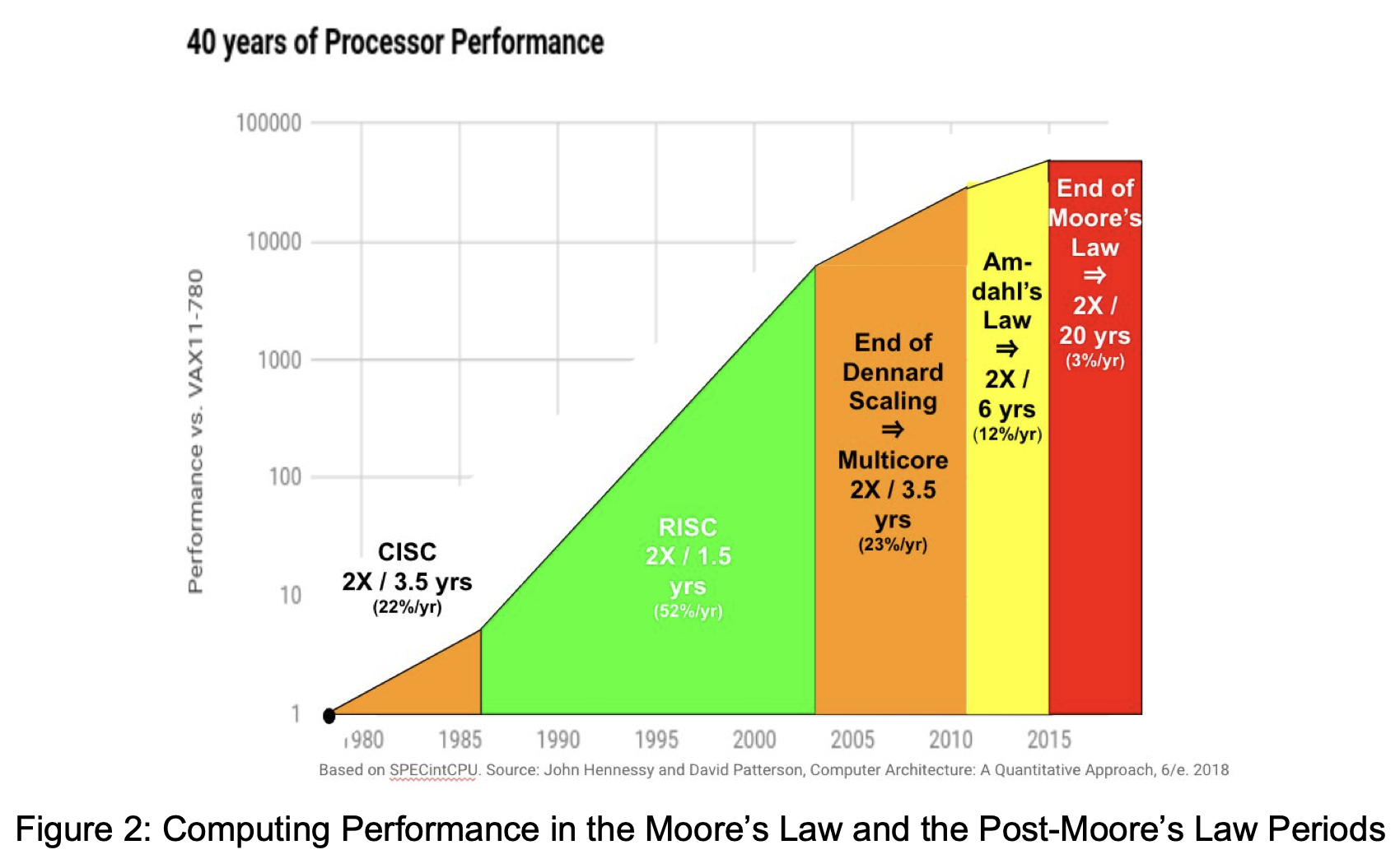 Degradation in the reliability of chip performance scaling under different regimes [14]
The TPU falls into the broad classification of hardware accelerators, of which the marquee distinction is that it is specialized for certain computational domains, hence the name Domain Specific Accelerator. Whereas general purpose devices are designed to accommodate the maximum number of program shapes, specialized designs are defined as much by what they can do as what they can’t. They trade off generality for performance. If we can’t rely on Moore’s Law and Dennard Scaling, and there are new workloads demanding attention, the goal is to optimize for the characteristics of those workloads and to discard everything else. Specialization asks what the optimal way to spend a fixed transistor and energy budget is to squeeze out performance.
Linear algebra is ripe for specialization because a relatively small set of parallelizable operations dominate neural networks. For the TPU that meant a monastic focus on those primitives. Neural networks are simple compositions of Matrix-Vector, Matrix-Matrix, and Elementwise computations over large tensors. Consider that matrix multiplication has cubic complexity. While computationally expensive, this one class of operations is the spine for a large fraction of what is required for a neural network. This narrows the window of optimizations that need to be baked into silicon. Matrix multiplies have the property that as the size of inputs grow, the ratio of compute, O(n^3), to data access, O(n^2), improves [15]. If you can dedicate hardware to speeding up arithmetic and coordinating data movement you can exploit this, and the arithmetic properties are complemented by the runtime properties. Neural networks can be fully specified ahead of time. With clever planning a program can be entirely mapped out before an instruction is issued. There was rarely a need before to design, tape out, and deploy custom silicon. Free performance gains made the economics of simply waiting versus the cost of designing an ASIC a non-starter. The decline of hardware scaling made exploring these realities attractive.
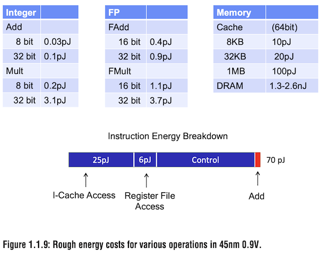 Horowitz Energy per Operation [11]
This opportunity is best exploited in the power budget. Compare the relative cost of arithmetic to control, memory access, and data movement. Horowitz [11] notes that over 50% of processor die energy is dissipated in caches and register files. These inefficiencies exist to mitigate the even greater inefficiency of large memory accesses. In [12] they cite that the energy to fetch and interpret instructions is 10-4000x more expensive than to perform simple operations. Moving and accessing data costs significantly more power, and what is required of deep learning is more arithmetic per unit control. Finding ways to circumvent relative power inefficiencies with specialization means rearchitecting chips to remove that waste.
The Inference Chip
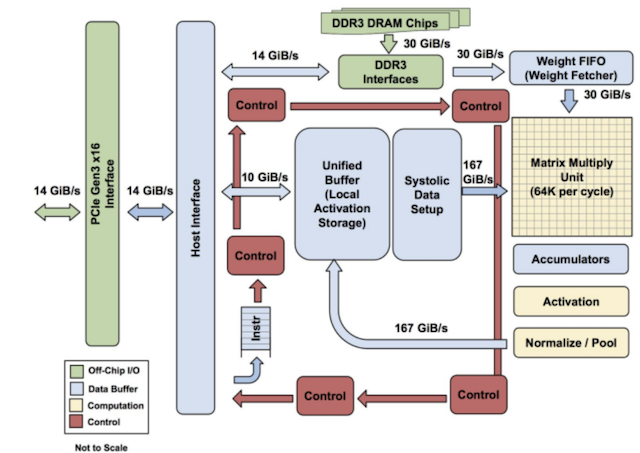 Block diagram of TPUv1 [1]
Datacenter expansions plans are a hell of a drug. To stem the tide of models devouring datacenter capacity, the first ASIC needed to focus on inference. Inference only needs a forward pass through the neural network. A simple neural network layer might look like this:
$$ ReLU( (X \cdot W) + b ) $$
Where X and W are input data and model weights, ReLU is a non-linear activation function, and b is a bias term. A matrix multiply followed by some elementwise addition and an elementwise maximum function. Imagine that chaining a handful of these layers together forms the totality of an inference. This simplified view on early model architectures gives us the general template for designing TPUv1. Matrix multiply, some activation looking functions on that result, feed the results to storage, repeat. To meet the initial deadlines the TPU design exploited this loop-like behavior.
TPUv1 is a single-threaded co-processor connected over PCIe with a 24MiB software-controlled Unified Buffer, an 8-bit integer systolic array, and 8GiB DDR3 DRAM. The device runtime lays out tensors, plans memory transfers with a programmable DMA controller between the host and the Unified Buffer (on-chip SRAM), and tiles compute operands. The host sends 12-bit CISC instructions to the device’s instruction buffer which the in-order sequencer consumes to move data to DRAM and issue MXU ops. The datapath consumes ~2/3 of the die area of the chip [1]. Take care to notice what it is not. It is not a multi-level cache hierarchy. There is no multi-threading or branch prediction or prefetching or TLB. The systolic array executes arithmetic and the runtime eliminates control overhead. TPUv1 is a spartan device aimed at making inference fast.
The heart of the device is the Matrix Multiplication Unit (MXU). It is a 256x256, 2D weight-stationary systolic array of processing elements, in this case MACs. The MXU targets dense GEMMs to maximize arithmetic intensity. The TPU is designed to keep the MXU busy. You can find nice animated demonstrations of data moving through the systolic array here or here.
MXU Cycle Timing
We’ll start with a simplified 4x4 systolic array. Although there are design variations of systolic execution [18][36], we are concerned with the 2D weight-stationary variant. The weights are pre-loaded into the array from the right hand side (the top in this diagram), and the inputs stream in from the left hand side (conveniently on the left). Once the weights are loaded they sit resident in the MACs, one weight per MAC. As the inputs flow from left to right, the MACs compute the product of the resident weight and the streamed input each cycle. The result of that computation is passed downward to the next processing element. If a MAC has one of these partial sums, it adds it to the result of the weight/input product and passes that new sum downward. At the bottom edge of the array there are no more computations and the result is passed to a 4096 row x 256-element bank of 32-bit accumulators.
MXU Double Buffering
Notice that weight pre-loading doesn’t happen all at once. It would waste cycles to wait for each MAC to have a resident weight before streaming in inputs. Weight pre-loading instead happens diagonally, with the left-most part of the systolic array receiving weights first. When the left column of processing elements has weights, the inputs begin streaming diagonally top to bottom. This imposes significant timing coordination for such a simple component. Much of the rest of the chips’ design can be thought of as accommodating these timing needs, and a particular instantiation of that is the liberal use of double buffering.
MXUs can perform immense amounts of arithmetic, but data movement/control stops at the edges of the systolic array. Between processing elements there is only result-passing with chains of two-input adders. If either weight or input data is not where it needs to be, stalls burn cycles that hurt MXU utilization. Spelling it out:
- The MXU holds two 64KiB tiles of weights with one reserved for double buffering
- Four 64KiB weight tiles act as a FIFO queue to decouple memory accesses and weight loads between DRAM and the MXU
- The Unified Buffer stores intermediate results from the accumulators and prepares new data to feed to the systolic array
- The bank of accumulators logically splits 4096 rows into two chunks of 2048 rows, one to feed outputs and one to drain them
Sizing the MXU
The number of processing elements that touch data before it reaches the accumulators grows quadratically with the array size which affects the speed of the computation. For a 256x256 array that is 65,536 MACs vs. 262,144 MACs in the 512x512 configuration. During fill/drain you pay an O(num_edges) cost to populate the buffers. Fewer edges better amortize this overhead. As arrays shrink they are penalized by wiring constraints. They perform less compute per data access and require running many wires between components. Sizing this device is a delicate balance between compute intensity and layout constraints, which we will see again in later generations.The runtime knows how long each operation it issues should take, so it can intelligently overlap them with one another. During matrix multiplications the UB prepares the next batch of inputs, the fixed activation units operate on the results in the accumulators, and the Weight FIFO banks more weights. Matrix multiplies are relatively long latency, which leaves lots of cycles between when work starts and when work ends. The runtime schedules memory accesses, data movement and computation deterministically to minimize stop-the-world pauses rather than make coordination dependent on the MXU. Hiding latency with overlapping improves parallelism, improves data reuse, and conserves energy otherwise wasted in control flow.
The headline figures from their paper are anachronistic by now, but they help contextualize the accomplishment of the first gen chip. 25x as many MACs and 3.5x the on-chip memory of the K80 GPU. 15-30x the inference speed and 30-80x the perf/W of the K80 and the Haswell CPU [1]. The fixed-latency, software-managed design created a hardware accelerator that eschewed prevailing designs that spent energy in cache hierarchies and control overhead. Maniacal focus on mitigating inference bottlenecks with large SRAM and coordinated data movement proved that TPUv1 worked.
The Training Chip
Neural networks need to be trained before they can be used for inference, and TPUv1 was not designed for training. Requirements include backpropagation to modify weights during execution, gradients with higher precision than int8, and support for diverse activation functions. This costs orders of magnitude more FLOPs [2], and those FLOPs must be distributed over multiple devices while maintaining deterministic execution. TPUv1’s fixed activation units were not flexible enough for experimenting with new algorithms. The memory subsystem was not flexible enough to coordinate work between multiple devices. The UB was not flexible enough to tuck more Matrix-Vector work in behind the MXU. The whole device was too tightly coupled. Adding that flexibility, without reverting to a general-purpose processor, needed a radically different datapath.
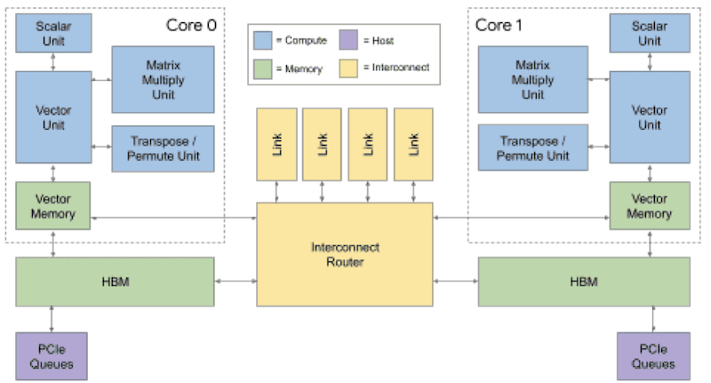 TPUv2 Block Diagram [2]
TPUv2 was animated from the bones of TPUv1, but only the MXU feels familiar. TPUv2 is a dual-core chip. Each core pairs a scalar controller with programmable vector units, local SRAM, a 128x128 MXU, and HBM. It adds inter-core interconnects (ICI) to communicate between the memory systems of each core and across chips. Two 128x128 MXUs combine to total the same 256x256 array from TPUv1 but simplify the circuit design. Unequal logic, wire, and SRAM scaling on smaller process nodes made arithmetic improvements comparatively free, enabling the chip designers to focus on the laggard scaling axes [2]. For the second generation MXUs that meant two efficiencies over their predecessor: BrainFloat16 and wire routing.
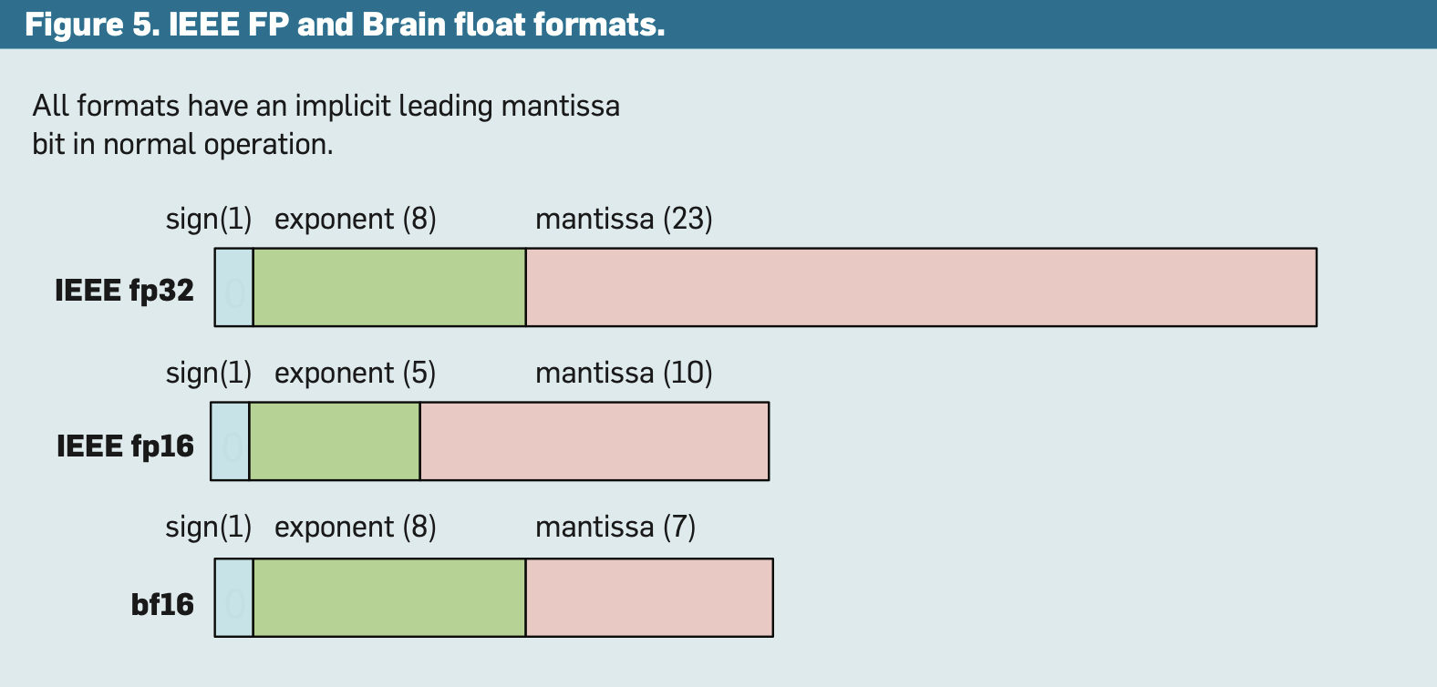 BF16 floating point format [3]
Dynamic range matters more than precision for neural network training. Gradients represented as integers don’t produce adequate convergence behavior; you need floating point numbers to make fine-grained weight updates. Accessing higher precision numerics however means sacrificing die area. Logic circuits need more adders to handle mantissa bits. Floating point adder arrays scale as (M+1) * (M+1), where M is the size of the mantissa, – 576 adders for fp32 and 121 adders for fp16 [14] – totalling more die area and more energy spent on arithmetic. Notice that although bf16 is the same number of bits as fp16, the proportion of exponent bits to mantissa bits is higher. bf16 only requires 64 adders in the MAC circuitry, and less circuitry means more MACs in the same package and power budget [2][14].
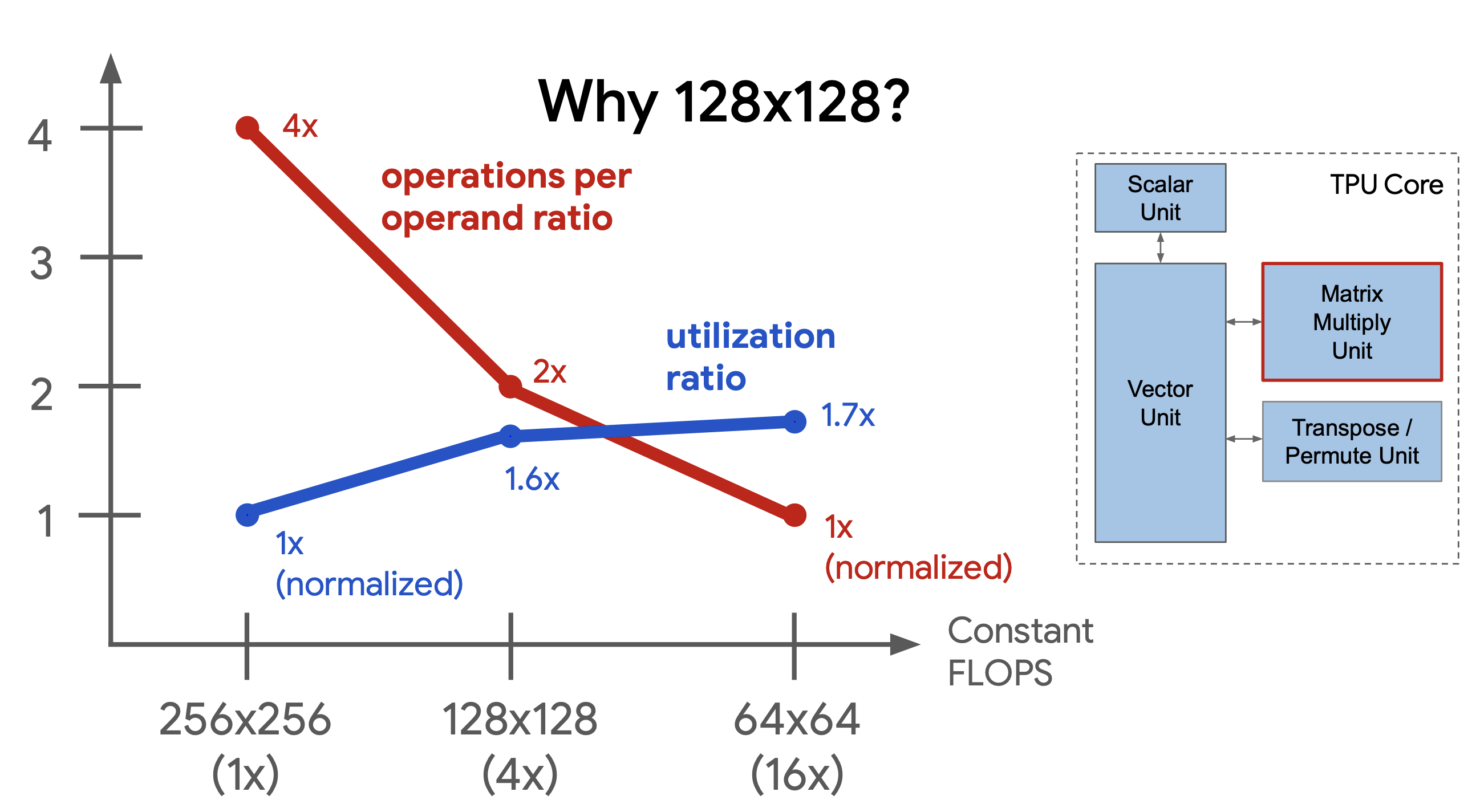 MXU Sizing Considerations [32]
Chip geometry considerations extend beyond individual processing elements. Big cores need long, global wires routed to/from functional units, FIFOs, and control units. Though wire diameters shrink on improved process nodes, their resistance and capacitance scale unevenly. Long wires are chunked into shorter segments connected with repeaters, but this induces signal delay making circuit timings more complex [5]. MXU configurations with multiple smaller cores shorten average wire lengths but need wires routed all over the chip. The trade off is between compute bandwidth and array utilization. Compute utilization scales down quadratically with the array area, but smaller arrays use more energy-efficient wires. Splitting the die into two cores and running fewer, shorter wires to the vector and control units balances wiring scaling with utilization.
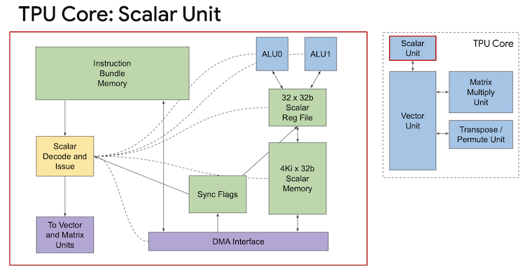 TPU Scalar Unit [32]
All those wires have to lead to somewhere. To drive the new datapath, TPUv2 introduces the scalar unit. When a user submits a program, the XLA compiler performs static analysis, lowering the program into 322-bit VLIW instruction bundles. XLA schedules DMAs, vector ops, and MXU work in a deterministic stream. The complexity of organizing program control flow is absorbed by software, keeping the scalar unit relatively simple. It is single-threaded and contains 4KB of scratchpad SRAM (SMEM), small instruction memory (IMEM), and a 32 element, 32-bit register file (SReg) connected to a dual-issue ALU. Sync registers flag when arithmetic and memory blocks are busy to explicitly synchronize execution. The host sends instructions over PCIe to HBM, where they are DMA’d into the Scalar Unit’s IMEM as overlays. Scalar instruction slots execute locally, and the vector/matrix slots are decoded and dispatched to the VPU/MXU [3]. There is no dynamic runtime scheduling, just instruction fetch, decode, and forward.
Two programmable vector processing units (VPU) consolidate the fixed function blocks from TPUv1. The VPU is a 2D SIMD processor designed to increase the ratio of vector operations to matrix operations. Each VPU has 128 vector lanes with 8 sublanes. Each sublane is connected to 32 dual-issue ALUs with lane-local register files (Vregs). The VPU is backed by 16MiB on-chip Vector Memory (VMEM) that mediates data movement to the MXU with pushes/pops onto a Result FIFO [3]. Each core’s VMEM has local access to half of the chip’s HBM, and DMAs to VMEM are strided to fetch contiguous tiles of data rather than issuing many small DMAs. The VPU accesses VMEM with explicit loads/stores to Vregs which remove the need for a cache hierarchy.
The simplicity of describing the rearchitected datapath belies the complexity that the subsystems represent. Whereas general purpose devices use branch predictors, TLBs, Out of Order execution, and a bevy of techniques to shuttle data and instructions, the TPU routes around a cache-centric design with software-managed execution. The aforementioned general purpose mechanisms alleviate runtime dependencies at the expense of more hardware and more energy. Control and caches consume massive amounts of the limited energy budget, so redesigning this subsystem is the difference between an economic chip and a renegotiated contract with power providers. When you know what operations you need, the order you need them in, and the operational characteristics of the hardware, you can move control flow to compile time. The VPU and Scalar Units are co-designed to leverage this operating paradigm, moving program orchestration to software.
Sample VLIW Instructions
VLIW instructions expose this complexity. They contain slots for 2 scalar, 4 vector, 2 matrix, 1 miscellaneous, and 6 immediate instructions [3]. Slots map to scalar/vector/matrix arithmetic, loads and stores, DMAs, synchronization flags, and data literals. Though innocuously named, the miscellaneous slot controls heaven and earth. It is reserved for kernel launches, DMAs, and synchronization guards which we can think of as WAITs. Data dependencies must be carefully sequenced to ensure operation A finishes before operation B uses its results. XLA utilizes the misc slot to keep subsystems working while guarding against illegal instruction sequences. Operational latencies are known constants at compile time, and XLA can use those values to place WAIT instructions at exactly the right point in the VLIW stream to minimize stalls.
Simplified TPU Instruction Overlay
Subsystems operate with different latencies: scalar arithmetic might take single digit cycles, vector arithmetic 10s, and matrix multiplies 100s. DMAs, VMEM loads/stores, FIFO buffer fill/drain, etc. all must be coordinated with precise timing. The MXU might be busy executing a matrix multiply for 128 cycles, meanwhile the VPU is preparing the next tile of weights for the Result FIFO. While DMAs prepare new data for VMEM a DMA_OVERLAY instruction gets inserted to fetch new instructions for IMEM. When the MXU finishes a tile, the hardware sends a signal to clear the MXU_BUSY bit in the scalar unit’s sync registers. When the scalar unit evaluates a WAIT_MXU instruction it sees that the bit is unset and hops to the next instruction for decoding. The scalar unit JUMPs to the new VLIW bundle region and the program continues. Seamlessly overlapping the work of an arbitrary DAG requires extraordinary co-design between the device and the software.
Decoupling the hardware gave software the capacity to drive massive data and instruction level parallelism. VLIW slots can launch 8 operations per cycle. That is 2048 vector ALUs and two 128x128 systolic arrays with minimal control overhead. HBM, VMEM, Vregs, and the MXU all remain busy with the same pipelining and overlap philosophy from TPUv1, only now massively scaled up. XLA wrests power away from control and back into the arithmetic units with coordinated, deterministic execution. Determinism across devices requires explicit communication between chips.
ICI forms the backbone of the training pods. It creates a coherent communication fabric that lets chips operate locally while composing into a mesh of devices acting as one large core. Two on-chip ICI links route data between the HBM and VMEM of each core. Four 496Gbit/s bidirectional off-chip links connect a TPU to its neighbors in the rack with OSFP passive copper. RDMAs over this fabric let chips treat remote HBM as explicitly addressable endpoints. Racks arrange 256 chips as a 16x16 2D torus over ICI to form the full supercomputer pod. ICI removes frequent host communication, skipping the cost of network cards, switches, and communication delays. All this sacrifices 13% of the die area for gains in distributing computations [3].
One dimensional torus wraparound
Let’s imagine that we’re playing a game of telephone. You and 8 friends are arranged in a 3x3 grid, and you can only communicate with your adjacent neighbors. Your goal is to send a message from the person at (0,0) to the person at (2,2) in the fewest messages. Many paths achieve this, but the shortest one is always four. Now imagine that the people on the left edge of the grid can wrap messages around to people on the right edge of the grid. This is logically like mirroring you and all your friends over that wraparound axis. These 3 new connections make our shortest path 3 instead of 4.
Logical mirroring in two dimensional torus wraparound, adapted from [5]
ICI plays this game of telephone in two dimensions. During backpropagation and optimizer state updates intermediate values accumulate across different partitions of the model located on different chips. Results must be broadcast to all the chips participating in the computation for synchronization. Whereas on-chip work is explicitly synchronized with hardware flags, work across chips is implicitly synchronized with MPI-style collectives (All-to-All, AllReduce, etc.). Torus topologies improve communication bandwidth and increase access to different communication patterns during synchronization.
32 wraparound links at 496Gbit/s enable 15.9Tbit/s of bisection bandwidth [3], which tells us how much data can move through the network. In a 4x4 array, a cut down the middle would sever 4 connections. That same cut down the middle of a 2D torus severs 8 connections. Even if each connection carries the same amount of data, there are more paths for data to move through which helps reduce congestion. XLA absorbs the complexity of cross-device scheduling. Software can trust that RDMAs will reach their intended stacks of HBM traveling along the ICI interface.
The same DNA ostensibly runs through TPUv1, yet the chips look and feel utterly different. The microarchitecture, software, and networking each became independently sophisticated parts of a larger system. Subsystems decoupled from one another yet still composed neatly. Where TPUv1 tightly choreographed everything, TPUv2 divided components into independent, asynchronously operating units communicating through explicit queues and synchronization points. TPUv3 was a minor revision in comparison. It has two MXUs per core, an increased clock, double the HBM capacity with 30% higher bus speeds, higher ICI bandwidth, and scales up to a 1024 node liquid-cooled rack. The dies only increased 6% relative to TPUv2 because engineers learned how to better lay the chip out [3]. Scaling the system to meet the continued growth of neural networks pushed future designs into new territory.
Scaling Up
As the footprint of the system grew, so too did the complexity of operating it. Our focus up to now has emphasized chip-local comparisons, e.g. How expensive are these operations relative to one another? How does the memory hierarchy work? How do subsystems A and B communicate on-device? While the TPUs remain the atom of the supercomputer, as we zoom out we observe the crystalline structure of the racks and pods. The fourth generation TPU is better examined thinking about memory as one unified domain. Specialization forces care in the microarchitecture, but the questions change. Where are collectives slow? How are larger tensors handled? Can we scale the racks further? Viewing the world from low altitude we find that TPUv4’s design emphasizes system scaling and energy management.
Peeking behind the accounting curtain for a moment, they note that “most OpEx cost is for provisioning power and not for electricity use, so saving power already provisioned doesn’t improve TCO as much as one might hope” [5]. Total Cost of Ownership (TCO) tries to consider the all in cost of the pods. On the back of a napkin we break this out into CapEx (equipment, installation, etc.) and OpEx (personnel, maintenance, power, etc.). Initially CapEx might dominate ASIC design, but as the platform matures, thinking through operational requirements produces different sets of optimizations. The need for fast, power efficient devices remains but extends out into the unknowable future. As model demands increase, better economics need compositional scalability in an efficient power envelope.
A brief note: TPUv4 is the training design and TPUv4i is the inference design. The impetus was to keep training and inference chips nearly identical so that there weren’t two separate designs awkwardly diverging into separate projects [5]. The relevant change is that the inference chip has one core while the training chip is dual-core.
Simplified Model of TPUv4 Systolic Execution
Fourth generation chips keep TPUv3’s MXU footprint, totaling 4 MXUs per core. In previous MXU designs partial sums moved downwards each cycle through a series of N two-input adders, where N is the size of the array, before reaching the output accumulators. TPUv4 batches groups of four products before passing them to custom 4-input adders. Batching products reduces the length of the adder chain from N to N/4, quartering the operational latency. Above we see 12 PEs bank four multiplies to reduce hops from 12 to 3. The specific implementation of these circuits isn’t clear from the paper, but this should provide enough motivation to understand the change. This circuit design decreases die area 40% and reduces peak power 12% [5].
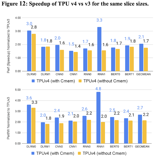 CMEM Speed Ups [4]
Accessing DRAM is still expensive, and inference workloads underutilize chips. TPUv4 adds 128MiB shared CMEM that is like an L3 cache but with the niceties of software-managed programmability. CMEM helps to keep all 4 MXUs busy with computations at the cost of 28% of the TPUv4 die area. On the 7nm process node, SRAM memory accesses are 20x more energy-efficient than DRAM accesses [5]. CMEM’s memory bandwidth sits in between HBM and VMEM, but unlike HBM it can both read and write data. Expanding the memory hierarchy and keeping data closer to the arithmetic units allows XLA to cut out expensive trips to DRAM. During inference, prefetching model weights into SRAM for multi-tenancy drives higher utilization of chip resources that may otherwise be sitting idle. The ability to swap weights out from SRAM rather than DRAM makes paying the context switching cost feasible. All that die area and upfront CapEx gets amortized over the life of the chip in TCO so long as XLA can effectively leverage it. Contrary to the prevailing LLMs-everywhere paradigm, ad serving and recommendation models (DLRMs) run the world. SparseCores (SC) are built to accelerate these models at the cost of 5% die area and power [4]. The key features of these models are their usage of embeddings. Embeddings map data into enormous sparse matrices. Efficiently handling these sparse matrices requires clever strategies to shard tensors across devices and to make looking up the correct slice of data fast. Unstructured sparsity suffers massive memory traffic and imbalances between compute, communication, and data-dependent execution. The MXU is ill-suited to make progress on sparse workloads because they waste cycles on empty computations and don’t directly manage communication. SparseCores address this class of models with a “Sea of Cores” architecture designed to accelerate collectives and memory accesses [4]. SCs are segmented into 16 individual compute elements (tiles) near DRAM that support multiple outstanding memory accesses [4]. Tiles communicate over a data crossbar with one another and over the on-chip fabric to the rest of the device. A stream of CISC instructions enabling data-dependent communication gets issued by the processor’s core sequencer. The Fetch unit (8-wide SIMD vector processor, scVPU) reads data from HBM into 2.5MiB of sparse memory (Spmem), and the Flush Unit writes data out to HBM. Five on-board cross channel units (XPU) perform embedding specific operations. When embeddings are distributed across remote devices SCs leverage the existing ICI bandwidth to access remote memory. The dataflow looks as follows: SCs alleviate the need for the MXU to handle computation and memory traffic on sparse data. They remove the CPU/DRAM bottleneck and shift sparse phases off the MXU path. The cores issue many RDMAs across the global address space of the TPUv4 pods, speeding up embeddings based models 30.1x versus CPUs [4]. Dedicating a small amount of die area to the gather/scatter intensive DLRMs allows the device to be flexible and efficient under multiple algorithmic regimes.SparseCores
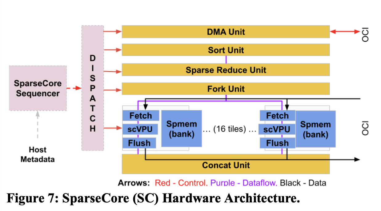 SparseCore Block Diagram [4]
Cores are getting crowded: MXUs, SparseCores, VPUs, HBM, and ICI routers. We see this component management pressure in the VLIW bundles. Driving the additional MXUs and CMEM required the VLIW bundle size to expand ~25% [5]. Adding new subsystems to the microarchitecture adds efficiencies that bubble up to system level performance, but lurking behind each of these changes is the specter of wiring. Fitting more efficient work onto the package with point-to-point connections became too great a tax. Training racks need to be close to one another in the datacenter to amortize the cost of cooling infrastructure, and this physical constraint forces the usage of optical fiber. ICI cabling in TPUv2/v3 coupled rack deployments so that a supercomputer couldn’t go into operation until the full pod was deployed [5]. To realize the TCO and energy wins of the microarchitecture system scaling needed to decouple and compose.
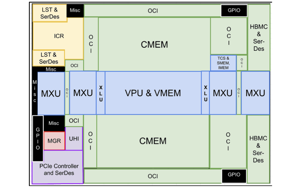 TPUv4i Floorplan [5]
The ICI needed to breathe. Previous revisions of ICI handled both on-chip communication and off-chip communication. More wires needed to be routed to/from the ICI interface as the number of components grew. This circuit layout pressure was complemented by the equally frustrating reality that handling on-chip and off-chip communication increased contention for ICI bandwidth. TPUv4 separates these concerns by adding a dedicated on-chip interconnect (OCI) fabric. The OCI interface handles data movement on-chip so that ICI can solely route traffic across chips. Notice in the fourth generation floorplan how much die area is reserved for OCI [5]. Shorter wires run between components and OCI rather than point-to-point. The OCI interface acts as the mailman. The Scalar Unit drops a message off at the OCI to submit a DMA to DRAM, and the OCI routes it to the memory controller. It tucks subsystem communication behind a unified data exchange interface that shortens wire routes and opens a path to flexible scaling in future designs.
Arbitrating memory accesses between HBM, VMEM, IMEM, SMEM and now CMEM meant maintaining too many sets of independent lanes. OCI uses 512B-wide native data paths segmented into four, 128B-wide groups across the memory hierarchy. Each group serves a quarter of the total HBM bandwidth (153GB/s) so that independent transfers don’t serialize behind one another [5]. Transferring small IMEM overlays shouldn’t have to wait on the completion of a long-latency tensor DMA. This partitioning strategy gives software more flexibility when scheduling work across a device. The full HBM bandwidth is available to each group, but software can schedule multiple concurrent transfers instead of funneling everything through one contested path. XLA plans large transfers to CMEM, CMEM feeds the arithmetic units, OCI handles message passing, and ICI routes and manages RDMAs. OCI and CMEM jointly help to improve spatial locality and reduce trips to HBM. TPUv2/v3 used two-dimensional, relaxed order DMAs to stride along two axes when moving data. This forced XLA to decompose complex tensor reshapes into multiple DMA operations. TPUv4(i) uses four-dimensional DMAs that stride along three axes moving 512-byte chunks [5]. Operations that previously required multiple round-trips to memory now happen in a single DMA. The architecture distributes DMA engines throughout the chip rather than centralizing them. Each engine acts as a co-processor that can decode and execute tensor operations independently. The unified design works identically for on-chip transfers, cross-chip transfers, and host transfers. XLA inserts explicit synchronization, but in exchange it gets predictable performance and the freedom to schedule data movement aggressively. The compiler knows the latency and pipelines around it.4D Tensor (R)DMAs
TPUv3 had already resorted to optical fiber across racks to enable the full 2D torus, but the 1024 node supercomputer could not expand its physical footprint. Rigid ICI wiring constraints meant individual racks couldn’t be used until each pod was deployed, and the system topology was fixed as configured unless a technician recabled the pod. Rack maintenance brought the whole pod offline with it. Optical Circuit Switching (OCS) infrastructure was the cure. Even though optical solutions are expensive, OCS optical components represent less than five percent of both system and power costs [4][10]. Centralizing cross-rack communications inserted massive programmability into the system. Substituting the cross-rack links with a programmable OCS provided massive gains in “scale, availability, utilization, modularity, deployment, security, power, and performance” [4], unlocking a new scaling paradigm.
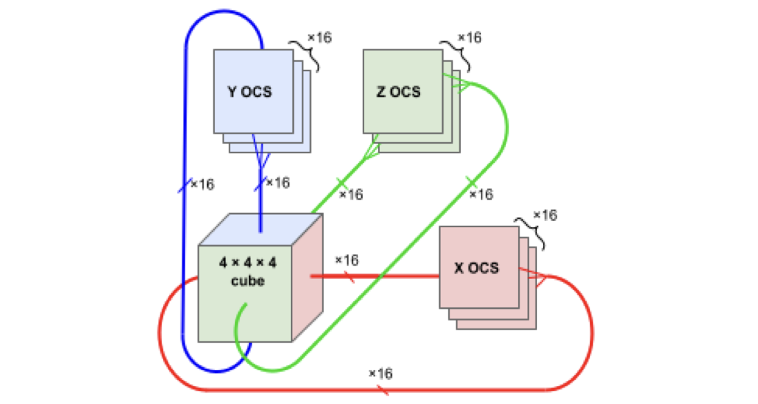 OCS Logical Diagram
Each rack in TPUv4 is a 4x4x4 cube, where this cube configuration is chosen to optimize all-to-all communications. Previous pod sizes (16x16 in v2, up to 128x32 in v3) were topology-limited. Devices could communicate between racks over ICI, but the system topology was statically programmed by the cabling. OCS removed these hard limits by centralizing cross-rack communication over an optical switching fiber. OCS offloads link establishment to an array of MEMS mirrors that dynamically configure links between devices in milliseconds [4]. New system topologies can be programmed on the fly by software, placing workloads on idle, non-contiguous machines. Dynamically reconfiguring the OCS improves system availability, tolerating outages in 0.1% - 1.0% of the CPU hosts [6]. TPUv4 pods scale up to 8x8 racks totaling a 4096 node cluster connected over OCS.
The OCSes isolate scaling complexity. Each rack contains 64 chips laid out logically as a cube. With 6 cube faces (+/- X/Y/Z), and 16 (4x4) chips per face, 96 optical links go to the OCS per rack. In the full 64 (8x8) rack pod, that is 6,144 uplinks to the OCS. This requires 48 OCSes that have 128 active ports to connect all the uplinks [4]. Moving cross-rack interconnects to a dedicated optical panel at this scale enabled programmable topologies, eased deployment by decoupling racks, and allowed software to effectively use OCS as a “plugboard” to route around node and link failures. OCSes use micro-electro-mechanical systems (MEMS) mirrors that tilt in three dimensions to steer optical beams. Each OCS contains two arrays of 136 mirrors. Each mirror has four voltage-controlled actuators that rotate it along two axes, steering light from any input port to any output port with sub-degree accuracy. Rather than monitoring each of the 136 mirrors with a dedicated photodetector, OCS uses a single camera per array with an 850nm monitoring laser. Image processing algorithms optimize the high-voltage driver signals to minimize insertion loss across the entire array. Once positioned, each mirror draws 10s of milliwatts to maintain alignment [10]. Circulators double the OCS’s effective capacity by enabling bidirectional communication. A circulator is a three-port optical device. Light entering port 1 exits port 2, light entering port 2 exits port 3. This cyclic property means a single fiber and a single OCS port can carry traffic in both directions simultaneously halving the required fiber count and OCS ports [10].Mirror, Mirror on the Wall
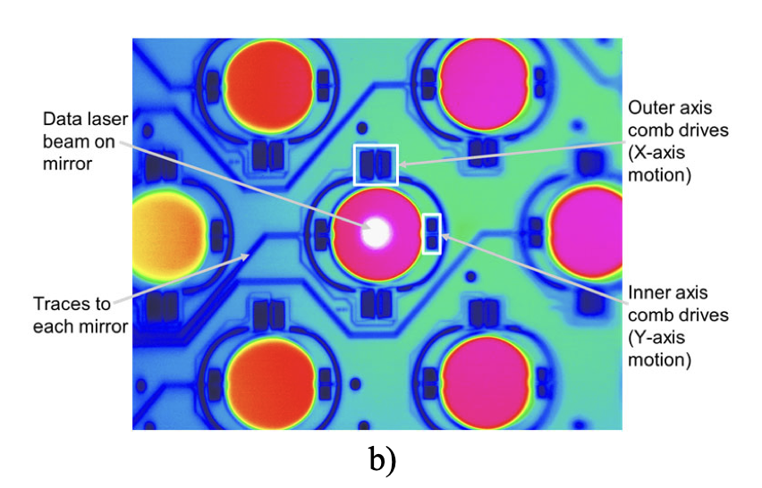 MEMS Mirrors [10]
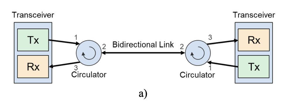 Circulators [10]
Full connectivity of the OCS across the pods meant that the torus topologies of the previous generations could now add a third wraparound dimension. The distance between racks was no longer a constraint, and since the OCS can program chip-to-chip connections on the fly a path to new topologies emerged. Not only could the connections between racks wrap around the z-dimension, they could twist.
Sample 1D Twisted Tori
We’ll make one modification to our previous wraparound topology diagram. Instead of wraparounds connecting only to the other side of their respective row/column, OCS programmability means that these connections can be offset. Adding twists to the wraparounds is an option not a requirement. Having the option to twist the network topology allows for new questions, e.g. given the communication pattern of this model, how should data be sent between participating chips? Twists make algorithmic experimentation and optimization two independently tractable targets and broadens the horizon of available efficiencies. Even without twisted topologies a third wraparound dimension adds bisection bandwidth to the network. The bisection bandwidth of 2D tori scales with the side length of the interconnects, N^(1/2). Adding the additional wraparound dimension scales bisection bandwidth with the area of the interconnects, N^(2/3). More paths in the topology shorten hops between participating nodes and alleviate system congestion along busy routes during synchronization. OCS better utilizes available devices and diversifies achievable topologies.
TPUv4(i) requires our thinking to broaden. We shouldn’t forget the impacts that microarchitecture improvements drive, but we need to consider the economics of the system holistically. Building warehouse scale solutions requires thinking about power provisioning, rack availability, interconnects, network topology, and accounting. Energy efficiency is still the overarching principle, but at datacenter scale. The message is simple: Target TCO over CapEx [5]. Adding CMEM is more expensive now but less expensive over time. Optical interconnects are expensive now but cost <3% of the fully operational system [4]. The duration of the design trade-offs became smeared into the future. All the same apparitions motivating TPUv1 go bump in the night, but they cast shorter shadows. TCO implies a system that requires operation, and the software that keeps the system available is an equal part of TPU’s development.
Island Hopping
Up to now we have enjoyed the quiet refuge of spreadsheet analysis, but the world is imperfect. Hardware dies, electricity spikes, and networks suffer congestion. The triumph of composing the system into decoupled, single responsibility units is not trivial, but infrastructure needs to serve real users. A cast of supporting software must keep chips available. Rock solid hardware relies on software to rationalize TCO obsession. The software is as much a part of the TPU story as the hardware.
We want to train a model. We decide which devices we need, pay rent, and start gawking at loss curves. When we submit our job for execution we don’t worry about the thousands of eager folks just like us. This mass of users vying for a fixed number of TPUs in sporadic intervals presents a problem. As the infrastructure provider what matters is that users don’t experience downtime. Components regularly fail and workloads are hard to predict. Once power has been provisioned every second of idle chip time or suboptimal workload allocation works against your best TCO approximations. Whether by underutilization or oversubscription, wasted resources are the enemy. Outer loop software that manages TPUs coordinates with XLA to find available nodes, check resource health, and configure ICI/OCS [6]. XLA needs to know which TPUs the computation will run on as well as the requested network topology because device placement is part of the program. Optimizing the system for high availability means dealing with the constraints imposed by ahead of time scheduling.
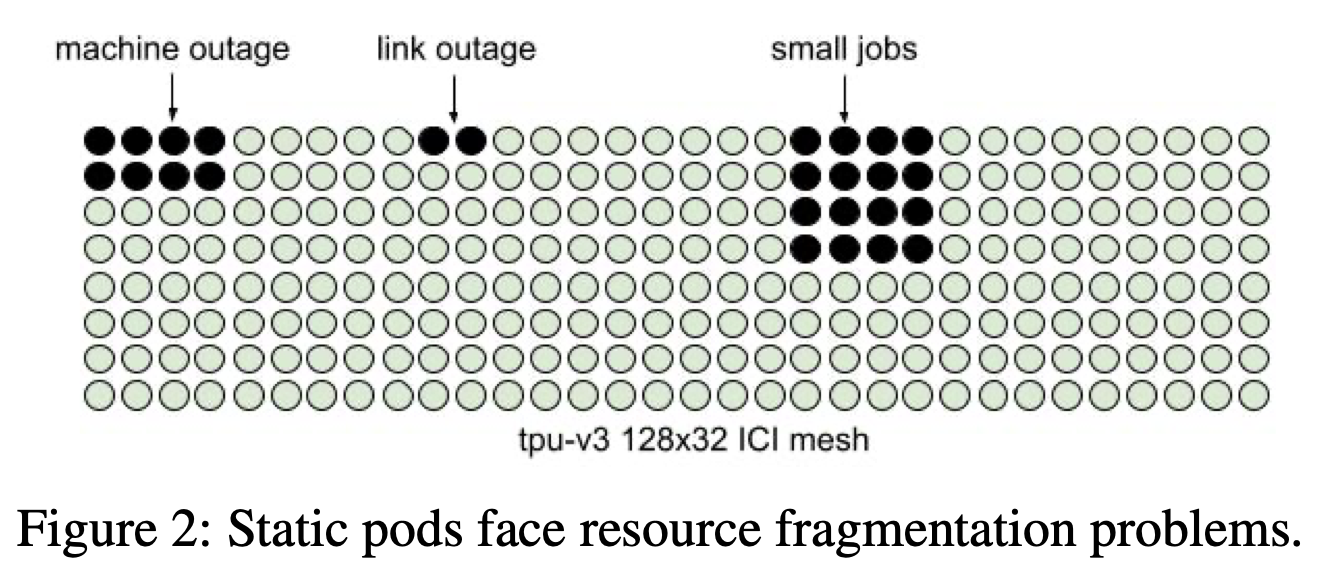 TPU Fragmentation [6]
Slices, Single Program Multiple Data (SPMD), and gang scheduling undergird TPU execution. Most workloads don’t consume an entire pod. Slices are declarations in code that allow developers to request an <X,Y,Z> device mesh which XLA uses to partition and shard models. This abstraction squirrels away both topology size and communication patterns. Pipeline parallelism may want a 2x2x1024 slice while data parallelism wants a 16x16x16 slice. The topology choice optimizes which communications are fast and which are slow. Mapping communications to a slice topology gives developers the freedom to experiment with parallelism strategies.
ICI coupling in TPUv3 meant the scheduler needed to find contiguous, healthy chips for workload placement. OCS lifted that restriction in TPUv4, but in both generations once a set of devices is selected the topology remains static for the duration of the program. A program owns the devices that it runs on until the program exits [8]. Concurrent users submitting unknowable slice sizes makes assigning devices like Tetris. The scheduler must place new jobs onto devices as old jobs pop in and out of existence. It needs mechanisms to rebalance suboptimal device allocations.
A single executable distributed to each participating device runs an identical program. SPMD encapsulates this many devices, single program framework. Developers write models as if they are running on one giant device, and the complexity of managing device-level data placement disappears from view. XLA’s partitioner rewrites every operation in the model to work on local tensor shards, inserting an AllReduce where gradients need to sync, scattering data where it needs to spread, and gathering results where they need to combine [7]. The single logical program becomes thousands of coordinated physical programs each operating on its local slice of data. Control is synchronized explicitly on-device with VLIW barriers and implicitly between devices by collectives. Gang scheduled execution means that each device launches the program all at once, trading off runtime resilience for performance. When a fault crops up during execution the job must be checkpointed and relocated [8]. The hardware stays simple, the software stays deterministic, but the orchestration layer must handle outages, link failures, and maintenance.
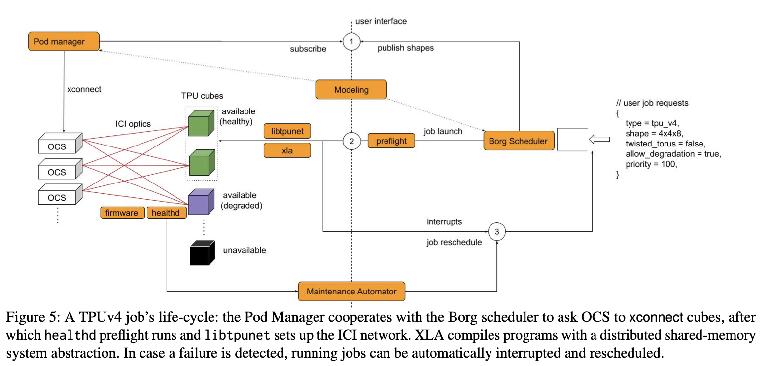 TPU Job Lifecycle [6]
Software must anticipate failures to juggle pre-allocated workloads. In [6] they note “To train a model, all TPU processes must be simultaneously up to synchronously update their weights via ICI collectives. A single failed, or interrupted process will interrupt the whole training process.” When a user submits a job, the cluster management client Borg queues it. If resources are fragmented or a job fails, Borg can preempt running workloads to shuffle them to different devices. When a job is ready to be scheduled, Borg selects a subset of devices and publishes an xconnect to the Pod Manager. The PM discovers pending xconnects and sends commands to the appropriate OCSes to connect the requested ICI channels. Once ICI connections stabilize, libtpunet configures the device’s ICI and programs its forwarding tables. XLA consumes the topology built by libtpunet to shard the model. Once execution begins, each device has its compiled program in local memory, knows its neighbors via ICI routing tables, and has its slice of the model weights in HBM. Thousands of devices execute in lockstep, synchronizing through collectives, without a single global runtime controller. The user does not see any of this background orchestration. Packets hop through a path of ICI switches and optical fibers to arbitrary pairs of TPUs determined by libtpunet once during setup. xconnects initiate mirror configuration in the OCS, triggering on-chip device managers to initialize physical connections between ICIs. When libtpunet issues an ICI session start it clears and rightsizes the ICI buffers in the data layer for new RDMAs. Routing is handled by forwarding tables that provide a simple abstraction to locate destination TPUs. XLA emits sets of RDMA operations called transactions for collective communications. On-chip DMA engines read data from HBM and send the data to the ICI’s transaction layer to send over the network [6]. All the required hardware for training drags down MTBF [6], so the system needs to be resilient to outages without bringing everything down. The system manages faulty links with fault tolerant routing. An offline integer linear program simulates link outages and frames the route selection as a max flow problem, using an all-to-all collective as the canonical use case. The results from the ILP are cached and accessible by libtpunet. Fault tolerant routing uses Wild First Routing as its heuristic. Packets can take a wild hop around faulty links before reverting to fault free routing. Though using fault tolerant routing may induce network congestion, TPU availability benefits [6].Fault Tolerant Routing
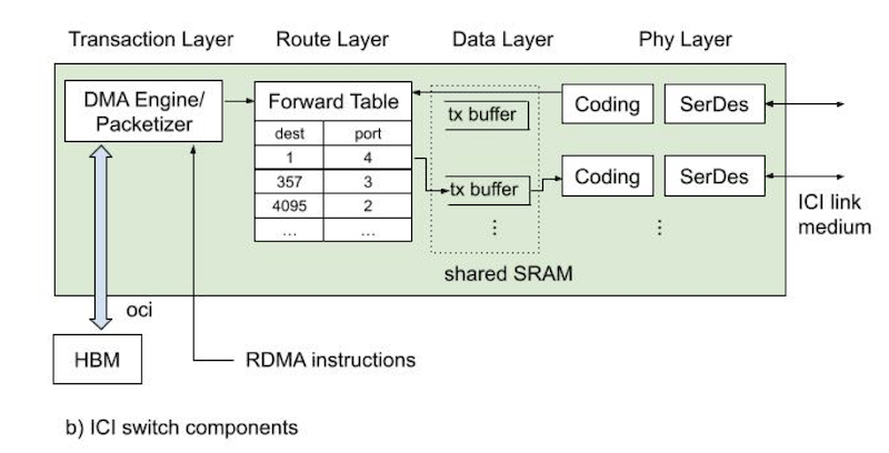 ICI Interface [6]
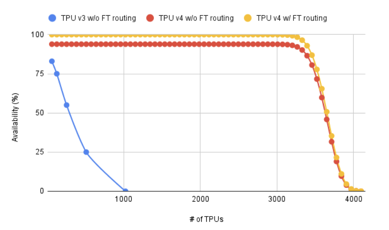 TPU Fault Tolerance [6]
Getting the whole system to cooperate at scale needs clear boundaries and hand-offs. Borg, PM, and libtpunet bless the configuration of the workload before triggering execution. When TCO skews towards operation, getting these pieces right is as important as systolic arrays and memory hierarchies. But this presentation of how the software works is also subject to the constant evolution of the TPU. Cores communicate over OCI. Chips communicate over ICI. Racks connect remote ICI links over OCS. That leaves us with one final communication frontier: the datacenter network.
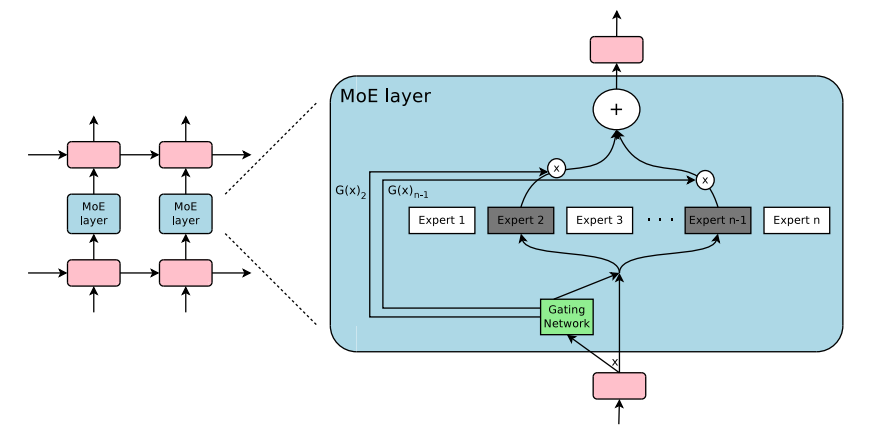 Mixture of Experts Routing [38]
SPMD assumes every device can communicate over ICI with predictable latency, which constrains developers to slice sizes that fit on a single pod. Islands of accelerators [8] leave idle capacity stranded across pods, and under contention, jobs struggle to get the right-shaped device allocation. Individual pods also constrain algorithmic flexibility. Unlike traditional transformers, Mixture-of-Experts models include runtime data dependencies. The gating mechanism in MoEs introduces non-deterministic routing during execution. The SPMD model has to be stretched to express the fine-grained, data-dependent control flow these models need. If you want to shard experts across pods there is no natural way to do so. Without the DCN there is no dynamic routing, resource sharing, or use of idle chips across pods.
The datacenter network (DCN) connects islands using Google’s Jupiter fabric [9]. From the TPU’s point of view it is the communication that doesn’t occur over ICI. Extending the many cores, one logical system scaling approach gets complicated by varying latency and bandwidth characteristics. Two solutions emerged from these limitations. Multislice extends SPMD across pod boundaries. It is a conservative but compatible approach with existing code. Pathways abandoned synchronous execution for asynchronous dataflow. It is more complex but necessary for true heterogeneity.
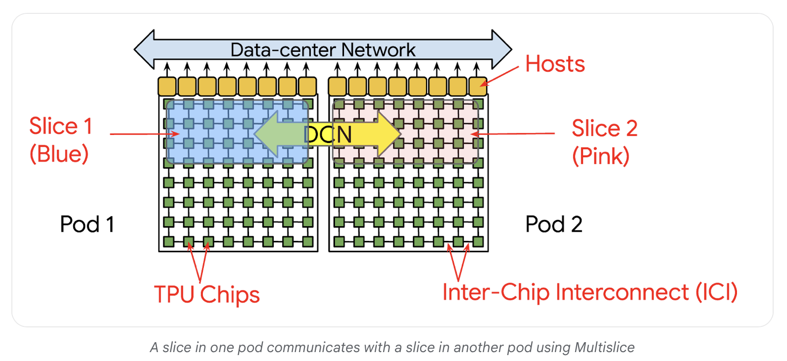 Logical diagram of Multislice over DCN [26]
Multislice extends existing SPMD code across pod boundaries with minimal changes. Pod boundaries are treated as just another level in the communication hierarchy. SPMD still uses gang-scheduled execution, but XLA understands that some collectives happen over ICI and others happen over slower DCN. The familiar declarative slice syntax adds a parameter to select devices across islands. The compiler optimizes collective placement to minimize cross-pod traffic. Multislice expands the number of devices available for training by providing access to resources across pods [26].
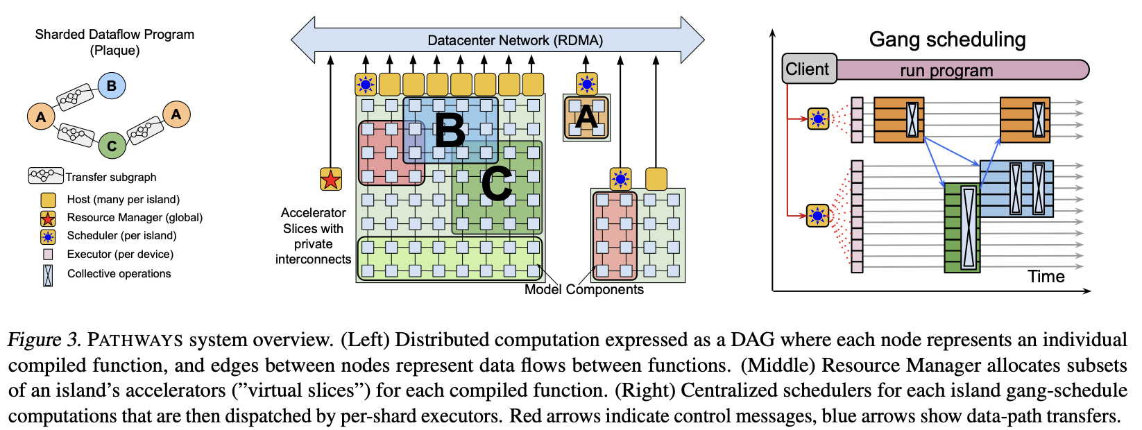 Pathways System Overview [8]
Pathways is a plug-in replacement for JAX’s backend that virtualizes the datacenter [8]. Instead of one giant SPMD program running in lockstep, it models execution as a DAG of compiled functions distributed across islands. Gang scheduling still happens within each island, but between islands coordination is asynchronous. There’s no single global runtime controller for the whole job. Mixture-of-Experts models can route activations dynamically to experts on different pods, and pipeline parallel stages can span multiple islands connected over DCN. Multiple programs can time-multiplex accelerators without context-switching overhead. Users request devices and the client compiles programs into a device-agnostic Pathways IR. XLA analyzes the program, the resource manager assigns physical TPUs, and the system inserts data movement operations between shards. Orchestration is complete by the time execution begins. Each device knows its program, its neighbors, and its slice of model weights.
Pathways uses a sharded dataflow model built on Plaque [8]. Each node represents a compiled function executing across thousands of TPU shards. The system uses parallel asynchronous dispatch. Pathways pipelines host side work in parallel instead of waiting for computation A to finish before preparing computation B. A control-plane scheduler per island enforces gang scheduling across programs. Between islands, Pathways uses centralized dispatch to coordinate placement and data movement. Data moves directly between accelerators over ICI within islands and DCN between islands. Pathways matches multi-controller performance by front-loading coordination work, even though cross-island dispatch is mediated by the control plane rather than issued independently by each host. This execution model performs as well as JAX and lifts restrictions on algorithmic expressibility [8].
A dedicated upstart could reproduce the hardware design philosophy, but the software co-design makes the TPU a mammoth. Borg allocates resources and preempts jobs. The Pod Manager configures optical switches. libtpunet knows every ICI routing edge case and manages fault tolerance. XLA compiles with full knowledge of topology and latencies. SPMD partitions models while maintaining the illusion of one giant device. Multislice extends that illusion across pods. Pathways rethinks distributed execution and virtualizes the datacenter as one programmable pool. Schedulers, compilers, and coordination systems all play one long song. Building a TPU competitor needs generations of hard earned experience points. Each new design reconsiders which approaches were dead ends. Admitting you were wrong and doubling back is the game. Thinking about the TPU is thinking about Everything Else.
Ceci n’est pas une TPU
After TPUv4 the well of detailed microarchitecture papers runs dry. You can still find information scattered across the internet, but not in the same succinct, curated way. Maybe more papers will be released publicly and we’ll be able to study these designs in greater detail, but until then we have to cobble together an understanding of our own. TPUv4 and v4i are followed by TPUv5p (performance) and v5e (efficiency), Trillium (v6e), and Ironwood (v7). We know that the inference (e) optimized designs retain a single-core architecture and use 2D tori instead of 3D tori. We know the interconnect and HBM performance numbers for the fifth, sixth, and seventh generation chips. We know that Trillium and Ironwood revert to 256x256 systolic arrays. We know that Ironwood scales up to 9,216 chips for training and 256 for inference with 1.77PB HBM that delivers 42.5 FP8 ExaFlops (6x Perf/W improvement over TPUv4) with a chiplet design for next generation reasoning and MoE workloads [16][20][21][23][24].
And I know that all of this fails to capture the totality of the enhancements since TPUv4. But a spec sheet like the one here or a primer like the one here could have told us that. The subsequent papers have focused on the system, but discussions of the system hide the simple origins of the device behind a hodgepodge of specs and new thundering heights. The essence of the thing becomes a folklorish amalgam of TPU lore. Myths are about meaning. Moore’s Law was never free in the literal sense. It required diligent engineering and enduring frustration, but decade after decade the compounding continued. The idea of Moore’s Law cast a spell that actualized its reality.
By nature the TPU is what it is not. The thrust and posturing of papers, talks, slides, and internet chatter focus on the technical minutiae, but the seams that hold this constellation of facts and figures together are the ordinary and the human. They are long emails and oscilloscopes in equal measure. How many of these choices go unseen? Hand-wringing about the system internals helps us to glimpse the creative act, but we mistake the painting for the paint chemistry. In this new world where nothing is free, every decision comes at an intentional, excruciating cost. The weight of the space of possibilities grows heavier knowing that each decision may foreclose another. Each choice is an act of reinvention in the face of a future that folds onto itself.
The TPU is an artifact born out of the quiet solace of steady hands doing careful engineering. AI DSAs are unlikely to be self-fulfilling in the same infinite feeling way as Moore’s Law. They will be five hundred ordinary decisions that compose into something greater. Can we make it smaller? Can we make it bigger? Can we make it easier to use? When we skim specs like the ones strewn above we notice the changes and feel the weight of what they represent. As new pressures get applied new entities emerge. For a moment we sense each decision branching into some unknown. Our new AI-obsessed world brings with it the demands of new ways of thinking. It is a reminder that the future is always at hand, and that if we participate in the myth-making we find that there are dragons after all.
References:
[1]: In-Datacenter Performance Analysis of a Tensor Processing Unit
[2]: The Design Process for Google’s Training Chips: TPUv2 and TPUv3
[3]: A Domain-Specific Supercomputer for Training Deep Neural Networks
[4]: TPU v4: An Optically Reconfigurable Supercomputer for Machine Learning with Hardware Support for Embeddings
[5]: Ten Lessons From Three Generations Shaped Google’s TPUv4i
[6]: Resiliency at Scale: Managing Google’s TPUv4 Machine Learning Supercomputer
[7]: GSPMD: General and Scalable Parallelization for ML Computation Graphs
[8]: PATHWAYS: ASYNCHRONOUS DISTRIBUTED DATAFLOW FOR ML
[9]: Jupiter Evolving: Transforming Google’s Datacenter Network via Optical Circuit Switches and Software-Defined Networking
[10]: Mission Apollo: Landing Optical Circuit Switching at Datacenter Scale
[11]: Computing’s Energy Problem
[12]: Domain-Specific Hardware Accelerators
[13]: The Accelerator Wall: Limits of Chip Specialization
[14]: The Deep Learning Revolution and Its Implications for Computer Architecture and Chip Design
[15]: Domain specific architectures for AI inference
[16]: How to Think About TPUs – Chapter 2
[17]: TPU Deep Dive
[18]: Understanding Matrix Multiplication on a Weight-Stationary Systolic Architecture
[19]: First in-depth look at Google’s TPU Architecture
[20]: WITH “IRONWOOD” TPU, GOOGLE PUSHES THE AI ACCELERATOR TO THE FLOOR
[21]: Ironwood: The first Google TPU for the age of inference
[22]: TPU Architecture – Google Documentation
[23]: Google Ironwood TPU Swings for Reasoning Model Leadership at Hot Chips 2025
[24]: Announcing Trillium, the sixth generation of Google Cloud TPU
[25]: A deep dive into SparseCore for Large Embedding Models
[26]: How to scale AI training to up to tens of thousands of Cloud TPU chips with Multislice
[27]: A Machine Learning Supercomputer With An Optically Reconfigurable Interconnect and Embeddings Support – HotChips Slides
[28]: Challenges in large scale training of Giant Transformers on Google TPU machines – HotChips Slides
[29]: Exploring Limits of ML Training on Google TPUs – HotChips Slides
[30]: Cloud TPU: Codesigning Architecture and Infrastructure – HotChips Slides
[31]: A DOMAIN-SPECIFIC TPU SUPERCOMPUTER FOR TRAINING DEEP NEURAL NETWORKS – Slides
[32]: Google’s Training Chips Revealed: TPUv2 and TPUv3 – Slides
[33]: A Decade of Machine Learning Accelerators: Lessons Learned and Carbon Footprint – MLSys Slides
[34]: Sparse-TPU: Adapting Systolic Arrays for Sparse Matrices
[35]: Systolic Array For VLSi
[36]: Why Systolic Architectures?
[37]: Doubly Twisted Torus Networks for VLSI Processor Arrays